Introduction to the Junction Field Effect Transistor (JFET)
In the expansive world of semiconductor electronics, the Junction Field Effect Transistor (JFET) stands as a fundamental building block. While most students and hobbyists begin their journey with Bipolar Junction Transistors (BJTs), the JFET offers a unique set of characteristics that make it indispensable for precision electronic design. As a voltage-controlled device, the JFET operates on principles that allow for high input impedance and low noise—features that are critical in the advanced communication and sensing technologies of 2026.
A JFET is a type of Field Effect Transistor (FET) that uses an electric field to control the flow of current. Unlike traditional transistors that require a constant input current, the JFET responds to voltage, making it incredibly efficient for specific applications like sensitive audio pre-amplifiers and high-frequency radio receivers. In this comprehensive guide, we will explore the internal construction, the physics of its operation, and the real-world applications that keep JFET technology relevant in the modern era.
The Core Construction of a JFET
Understanding how a JFET is built is the first step toward mastering its behavior in a circuit. The device is essentially a solid piece of semiconductor material with specific regions “doped” to create the control mechanism.
1. The Channel
The “Channel” is the heart of the JFET. It is the path through which electric current (charge carriers) flows from one end of the device to the other.
- N-Channel JFET: If the channel is made of n-type semiconductor material (where electrons are the primary carriers), it is called an N-Channel JFET. These are the most common because electrons move faster than holes, leading to better performance.
- P-Channel JFET: If the channel is made of p-type material (where “holes” are the carriers), it is a P-Channel JFET.
2. The Terminals
Every JFET features three distinct terminals that allow it to interface with a circuit:
- Source (S): This is the terminal through which the charge carriers (electrons or holes) enter the channel.
- Drain (D): This is the terminal where the charge carriers leave the channel. The current flowing from Source to Drain is the primary output of the transistor.
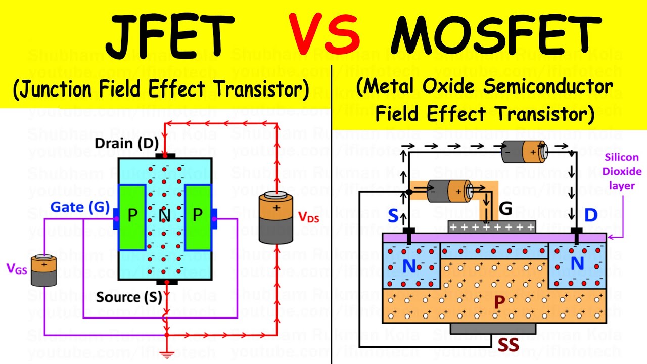
- Gate (G): The Gate is the control terminal. It is made of semiconductor material that is opposite to the channel material. For an N-channel JFET, the Gate is P-type. Its primary job is to create an electric field that regulates the current.
3. The Gate Structure and P-N Junctions
The Gate is not just a single point; it is typically placed on both sides of the channel. This creates two P-N junctions. These junctions behave exactly like diodes. By applying a reverse-bias voltage to these junctions, we can change the width of the channel, much like squeezing a garden hose to control the flow of water.
How a JFET Works: The Physics of Control
The operation of a JFET is all about the “Depletion Region.” When a P-N junction is reverse-biased, an area develops that is void of charge carriers. We call this the depletion region.
1. Condition: VGS = 0 (Gate at Zero Voltage)
When there is no voltage applied to the gate ($V_{GS} = 0V$), the depletion regions at the P-N junctions are very thin. The channel is wide open. If we apply a voltage between the Drain and Source ($V_{DS}$), current flows easily through the channel. In this state, the JFET acts like a simple resistor.
2. Applying Reverse Bias (The Squeeze)
In an N-channel JFET, we apply a negative voltage to the Gate. This negative voltage increases the reverse bias on the P-N junctions. As a result, the depletion regions grow wider and push into the channel. Because the depletion region has no free carriers, it cannot conduct electricity. This effectively narrows the conductive path, increasing the resistance and reducing the current flowing to the Drain.
3. The Pinch-Off Point and Pinch-Off Voltage ($V_P$)
As we continue to make the Gate voltage more negative, the depletion regions from both sides eventually meet in the middle. At this point, the channel is completely “pinched.” This is known as the Pinch-Off Point. The specific voltage required to reach this state is the Pinch-Off Voltage ($V_P$). Once the JFET is pinched off, the current reaches a maximum level (saturation) and stays constant even if you increase the Drain-Source voltage further.
4. The Cut-Off Region
If the Gate voltage is made even more negative than the pinch-off voltage, the channel is fully blocked. No current can flow from Source to Drain. In this state, the JFET is in the Cut-Off Region and acts like an open switch.
JFET vs. BJT: A High-Impact Comparison
Choosing the right transistor is crucial for 2026 design standards. Here is how the JFET compares to its Bipolar counterpart.
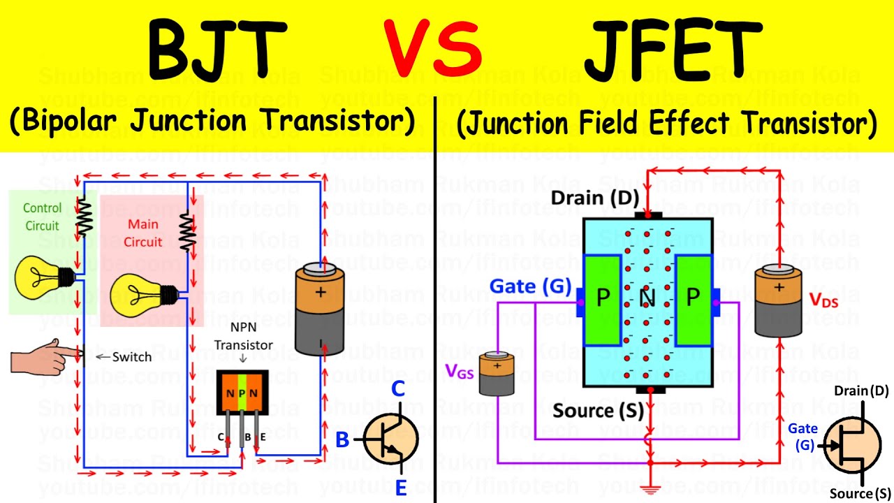
| Feature | JFET (Field Effect) | BJT (Bipolar Junction) |
|---|---|---|
| Control Parameter | Voltage ($V_{GS}$) | Current ($I_B$) |
| Input Impedance | Extremely High | Low |
| Noise Level | Very Low (Ideal for Audio) | Moderate |
| Thermal Stability | High (Negative Temp Coeff) | Low (Prone to Runaway) |
| Power Consumption | Minimal | Significant (Base current) |
| Charge Carriers | Unipolar (Only one type) | Bipolar (Both holes and electrons) |
Conclusion: The Future of JFET Technology
The Junction Field Effect Transistor remains a cornerstone of electrical engineering. Its ability to provide high-impedance, low-noise control via an electric field makes it a primary choice for designers in 2026. Whether it’s at the heart of a high-end audio mixer or serving as a critical buffer in a medical wearable, the JFET’s simple yet effective physics continues to drive innovation.
As we push toward 2030, the integration of JFETs into wide-bandgap materials like Silicon Carbide will only expand their reach into higher-power and more extreme environments. Understanding the JFET is not just a lesson in the past—it is an investment in the future of electronic design.