🎥 Watch this quick video explanation before reading the detailed guide.
Introduction to Transistors: The Building Blocks of Modern Electronics
In the vast landscape of electronic components, few inventions have had as much impact as the transistor. Since its inception, the transistor has replaced bulky vacuum tubes, leading to the miniaturization of computers and the birth of the digital age. Today, we focus on two of the most significant members of the transistor family: the Bipolar Junction Transistor (BJT) and the Junction Field-Effect Transistor (JFET).
Both BJTs and JFETs are semiconductor devices used to amplify or switch electronic signals and electrical power. However, they are not interchangeable. They differ fundamentally in their internal architecture, how they are controlled, and the specific roles they play in a circuit. Whether you are designing a high-fidelity audio amplifier or a sensitive sensor circuit, understanding these differences is critical.
Understanding the Bipolar Junction Transistor (BJT)
The BJT is the “classic” transistor that most students encounter first in their electronics journey. The term “Bipolar” refers to the fact that its operation involves both electrons and holes as charge carriers.
Construction of a BJT
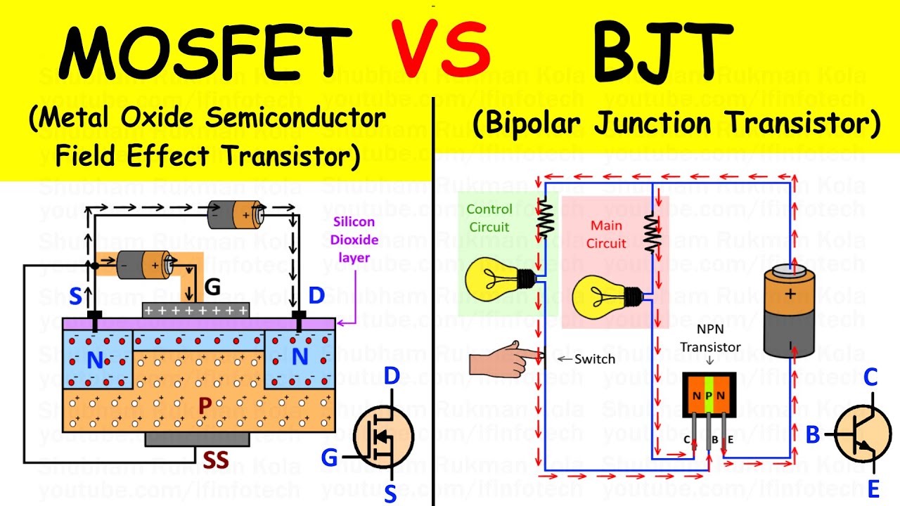
A BJT is constructed using three layers of semiconductor material. Depending on the arrangement of these layers, we get two primary types:
- NPN Transistor: A P-type layer is sandwiched between two N-type layers.
- PNP Transistor: An N-type layer is sandwiched between two P-type layers.
The BJT features three terminals:
- Emitter (E): Heavily doped to “emit” charge carriers into the base.
- Base (B): A very thin, lightly doped central layer that acts as the control gate.
- Collector (C): Designed to “collect” the charge carriers from the base.
Working Principle: A Current-Driven Device
The BJT is a current-controlled device. This means that a small amount of current flowing into the Base terminal controls a much larger current flowing between the Collector and the Emitter. Because of this high current gain, BJTs are exceptionally good at signal amplification.
Understanding the Junction Field-Effect Transistor (JFET)
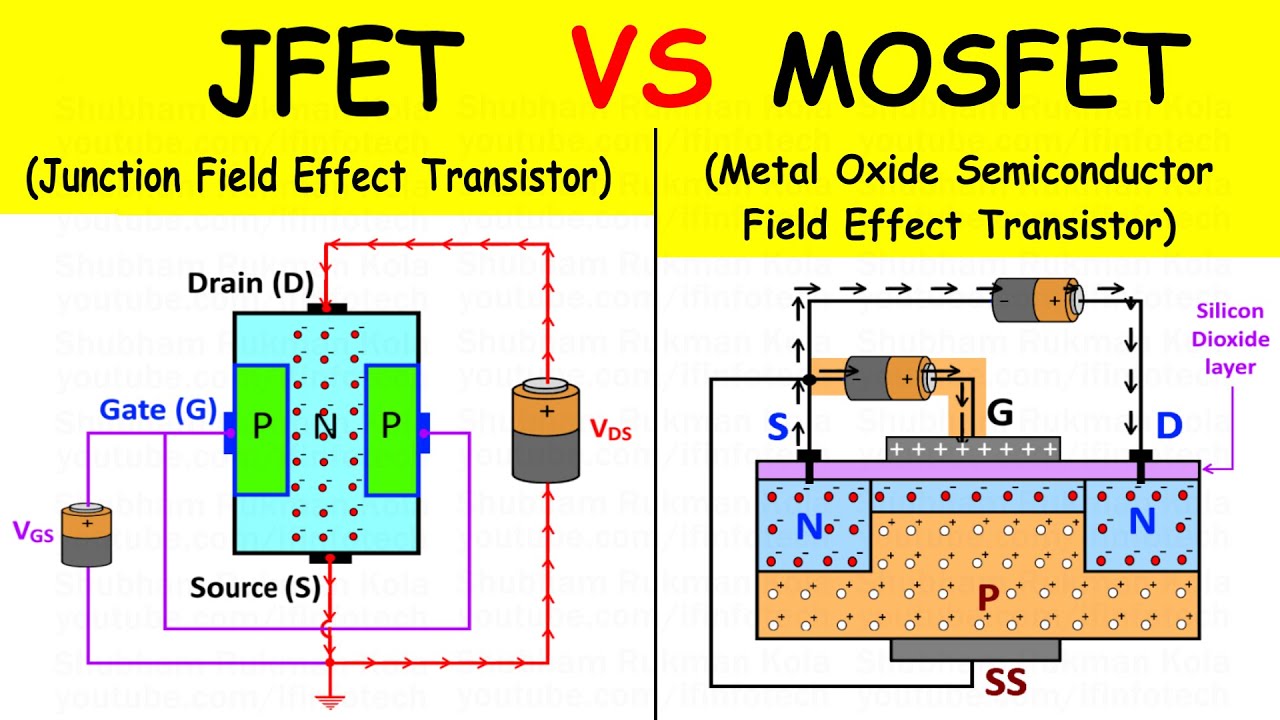
The JFET is a type of Field-Effect Transistor (FET) that operates using an electric field to control the flow of current. Unlike the BJT, it is a unipolar device, meaning it relies on only one type of charge carrier (either electrons or holes).
Construction of a JFET
A JFET consists of a “channel” of semiconductor material through which the current flows. It also has three terminals:
- Source (S): The terminal where charge carriers enter the channel.
- Drain (D): The terminal where charge carriers leave the channel.
- Gate (G): The controlling terminal that regulates the channel width.
JFETs come in two versions: N-Channel (most common due to higher electron mobility) and P-Channel.
Working Principle: A Voltage-Driven Device
The JFET is a voltage-controlled device. By applying a reverse-bias voltage to the Gate, an electric field is created that creates a “depletion region.” This region narrows the channel, restricting the flow of current between the Source and Drain. Ideally, the Gate draws zero current, which gives the JFET its most famous characteristic: High Input Impedance.
BJT vs. JFET: Detailed Comparison Table
| Feature | Bipolar Junction Transistor (BJT) | Junction Field-Effect Transistor (JFET) |
|---|---|---|
| Device Type | Bipolar (Uses holes and electrons) | Unipolar (Uses majority carriers) |
| Control Mechanism | Current-Controlled (Base current) | Voltage-Controlled (Gate voltage) |
| Input Impedance | Low (Draws base current) | Very High (Gate is reverse-biased) |
| Switching Speed | Moderate (Due to charge storage) | Fast (No charge storage effects) |
| Noise Levels | Higher (Shot and thermal noise) | Lower (Ideal for sensitive audio) |
| Thermal Stability | Lower (Prone to thermal runaway) | Higher (More stable with heat) |
| Power Efficiency | Lower (Needs constant base current) | Higher (Gate draws no power) |
| Common Use Case | High-gain amplification | High-impedance sensor inputs |
Conclusion: Choosing the Right Transistor
Both the BJT and the JFET have secured their place in the history of electronics. In 2026, the choice between them comes down to your specific design goals. If your priority is high gain and strong amplification, the BJT is your best bet. If your priority is low noise, high input impedance, and power efficiency, the JFET is the clear winner.
As semiconductor technology continues to evolve into wide-bandgap materials like Gallium Nitride (GaN) and Silicon Carbide (SiC), the lines between these devices may blur, but the fundamental principles of current vs. voltage control will remain a cornerstone of electrical engineering.
Watch the Full Tutorial: [Insert Video Link Here]
Frequently Asked Questions (FAQs)
A transistor is a semiconductor device used to amplify or switch electronic signals and power.
BJT is current-controlled, while JFET is voltage-controlled.
JFET has very high input impedance compared to BJT.
BJTs are used in amplifiers, switching circuits, and RF applications.
Because they produce less noise and have high input impedance, making them ideal for sensitive circuits.
![Junction Field Effect Transistor [JFET] Explained: Construction, Working, Application | Shubham Kola](https://shubhamkola.com/wp-content/uploads/2026/04/Junction-Field-Effect-Transistor-JFET-Explained-Construction-Working-Application-Shubham-Kola.jpeg)